Intel has a unique position in the semiconductor industry as the only major integrated design manufacturer (IDM), which means they design and manufacture their own advanced chips as one company. While Samsung has both capabilities, there is actually a firewall between LSI (by design) and the foundry. Intel's unique position as an IDM is both a major structural advantage and a disadvantage.
Today we want to talk about Intel's inefficiencies in terms of technology and cost.
In theory, by being a single company with fewer restrictions on data sharing, Intel could optimize each other's manufacturing and design more closely than rivals such as AMD and TSMC. Their final chip pricing can be lower than AMD because there is no external TSMC foundry tax to pay.
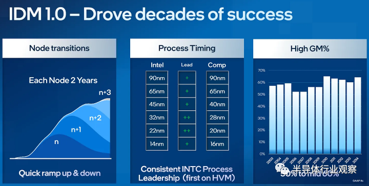
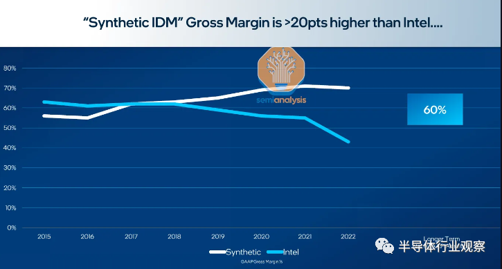
For decades, this model worked and has worked. Intel is ahead of all competitors at the process node and is therefore able to dominate. Their profit margins are consistently higher than companies like TSMC and AMD. The figure below shows what foundries + fabless companies and Intel would look like if they were assumed to be the same company.
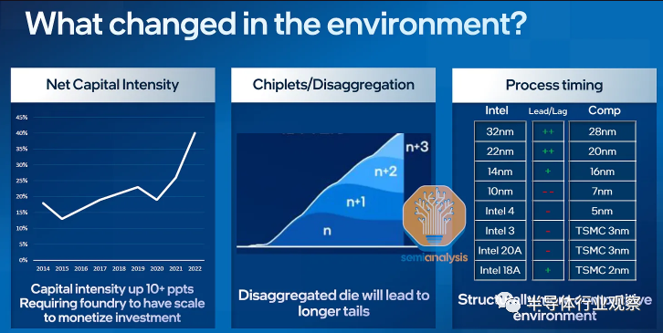
The process node advantage began to show cracks in the 14nm process in the early 2010s, but then completely collapsed during the transition to the 10nm process, which was scheduled for 2016. Foundries raced to lead in 16 nm, 10 nm and 7 nm processes, surpassing Intel's three-year lead and reversing the decline. Three years of deficit.
Some of these cracks are due to large IDMs. Responsibility and accountability are not properly implemented across teams and business units. Certain divisions of Intel gradually declined, falling behind the industry in terms of performance or cost, but no one could tell because Intel was in its own overwhelming engineering dominance.
Once Intel lost its lead, inefficiencies became apparent. Today, Intel makes wafers significantly less efficiently than TSMC. Due to low tool utilization and poor yield, Intel needs more fab space to achieve the same yield.
At the same time, Intel's design team was significantly behind AMD, requiring a larger core and more transistors, consuming more power to achieve similar performance. In addition, because of the poor design methodology, it took Intel's design team longer and more expensive to get the new architecture into production.
One of intel's solutions to these problems is to catch up with rival process nodes by shrinking two processes in quick succession (intel 4/3 and intel 20A/18A). But that alone won't solve the problem, as they still lack scale, customer base and operational efficiency.
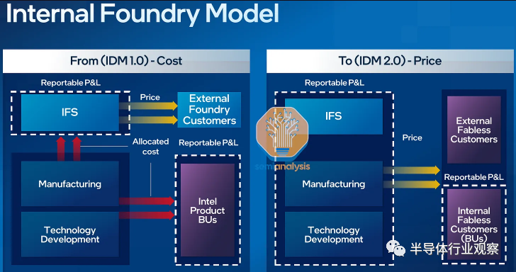
Intel is currently trying to solve many of these problems and transform itself into an external foundries for various external customers. While on the surface this only helps if they can win over external customers, there are other advantages.
By moving to an in-house foundry model, Intel can begin to end the pointless practice of assigning costs to entire business units rather than individual designs and teams. This will help address some of their major inefficiencies by reducing responsibility to a lower level, which will help manage costs at the product and fab level.
These various problems were overwhelming and led to the Intel we see today. In general, Intel product teams can hide behind their manufacturing prowess and ignore the costs that are allocated to the entire business unit.
In semiconductor manufacturing, wafers are manufactured in batches, called lots. These batches are collections of wafers that are processed sequentially by the tool before proceeding to manufacturing with the next available tool. Since a single fab costs tens of billions of dollars, it is essential to maximize the use of fab tools. In general, processing time for frontier wafers can take up to 10 weeks due to the batch of wafers.
On the other hand, if the cost is not considered, advanced wafers can also be processed in a few weeks, but this will cause the tool to constantly wait for the wafer to be processed as soon as possible, resulting in great inefficiency. This is called a "hot lot" and refers to a batch of wafers that are prioritized and processed faster than a standard batch.
"They can do any number of hot batches, they can do any number of samples," said David Zinsner, Intel's chief financial officer.
This could be for a variety of reasons, such as speeding up the validation of new process steps or tools, or creating test chips for new designs or technologies. The term derives from the idea that these wafers are "hot" because they are pushed into the manufacturing process as fast as possible.
"We do use a lot of 'hot lots'. Often, as a general manager, I don't always think as hard as I should about the cost of hot lots - not just the cost, but the disruption in terms of plant utilization and efficiency." Sandra Rivera, executive vice president and general manager of Intel's data center and Artificial Intelligence group.
However, running "hot lots" does reduce equipment utilization and overall fab efficiency. So it's a trade-off between the urgency to process a particular wafer quickly and the overall efficiency and throughput of the manufacturing plant.
"Our benchmark tests show that our materials are two to three times faster than industry peers, and we expect an 8 to 10 percent impact on total production." Said Jason Grebe, vice president and general manager of Intel's enterprise Planning Group.
Intel is solving this problem by moving to an in-house foundries model and charging business units for "hot lots" just as any other foundries charge customers for these "hot lots."
Intel believes this change alone could save them between $500 million and $1 billion annually.
The cost of designing chips is very high. Once a complete design is available, putting it into production requires sending the designs to a fab, converting those designs into dozens of physical photomasks to place inside a lithography tool, and running test chips through thousands of process steps. Once the test chips are received, they can be checked for errors/problems and the design can be adjusted.
But one of Intel's major disadvantages right now is that they require more iterations. Stepping means sending the modified design to the fab and creating a new photomask for the new test chip.
It took Intel 12 steps to bring Sapphire Rapids to market, while AMD typically takes only two to three steps to bring competing chips like Bergamo and Genoa to market. This makes it significantly more expensive for Intel to manufacture all those extra photomasks and greatly increases the time it takes to bring a new design to market.
We've even heard rumors from former employees that there was a time when some Intel design teams would rather send designs to the fab, get lots of samples back, and test them for errors, than get more done through simulation and validation.
Intel plans to address this problem by reducing the number of samples and steps by charging the design and product business units a fair price for these operations, rather than allowing an arbitrary number of steps. A few years ago, the design team began to shift to a design approach that was more in line with industry standards, although the task was daunting.
Intel believes this change will save them between $500 million and $1 billion annually.
Once the chips are manufactured, they are tested and classified to troubleshoot and make various classifications to go into different products. For many years, Intel has been a pioneer in testing, sequencing, and packing. Their tools are highly customized and have many unique internal test modes. While this gives Intel some advantages over the industry, it's not all positive.
"Our testing time is getting longer and longer compared to our industry peers. Currently, we estimate that our testing time is two to three times that of our competitors. In effect, our low-cost test bed is subsidizing the growth of our test time." Said Jason Grebe, vice president and general manager of Intel's enterprise Planning Group.
Once again, Intel's huge manufacturing advantage has turned into a disadvantage. Given that the field reliability of the final chip is not really differentiated, there is no need to test two to three times longer than competitors such as AMD.
Intel believes that charging business units more directly for testing, classification, and categorization will make them more aware of the testing strategies they use in their designs and save about $500 million a year.
In addition, Intel's advanced binning strategies led them to develop a product strategy that we call "SKU Spam." In the PC and data center space, Intel has dozens of SKUs because they are able to sort chips into the many boxes of final end-market chips. There is clearly potential for cost savings by reducing the number of SKUs compared to the much simpler product stacks of AMD, Broadcom, and Nvidia, but we haven't heard of any plans from Intel to change this.
Product managers and design teams used to use Intel's manufacturing capabilities to hide architectural inefficiencies. In an in-house foundry model, this changes because a product with a bloated chip size, such as Sapphire Rapids, will immediately impact the team's cost structure, rather than being gobbled up by the manufacturing organization. As a result, these changes will refocus teams on architecture, chip size, and the resulting costs.
Intel believes this will save more than $1 billion a year because teams can more easily determine which features are worth spending chip square footage on and which aren't. Currently, Intel's Sapphire Rapids spends a lot of square footage on features that most customers don't use.
The Intel design team also tended to ignore the mask challenges and lithography tool throughput issues that were manufactured in-house, which is why TSMC charges customers.
Intel did not say whether it would start charging in-house foundry customers for the effort. Intel is also very focused on ramp rates as a method of cost expansion. TSMC's biggest advantage is that their 7nm and 5nm high volume production has increased from 0 wafers per month to 50,000 wafers per month in 6 months. This allows them to identify and pass on benefit knowledge at an earlier time period over the remainder of the node's life cycle. It also improves tool utilization. It's worth noting that TSMC's 3nm capacity was even more negligible due to various missteps and cost issues, which led Apple to switch to a separate SOC approach.
If Intel wants to catch up, they need to be able to move up faster. Ice Lake and Sapphire Rapids ramp speeds are extremely slow, resulting in low capital utilization and slow yield learning. Intel will now charge internal teams a fixed wafer price over the lifetime of a node to try to speed up the production of new products, which according to Intel could both save $1 billion a year and increase the speed of getting competitive new products to market
Much like TSMC, Intel will also start charging teams access fees and locking in orders ahead of time. Their wafer orders to internal customers will also start to become less flexible. This change will help increase tool utilization as better production can be planned, which will also result in significant cost savings.
Overall, Intel has a lot to say about saving costs through various changes to its in-house foundry model.